filmov
tv
Lithography (Field Of Study)
0:07:44
‘Semiconductor Manufacturing Process’ Explained | 'All About Semiconductor' by Samsung Semiconductor
0:05:26
Photolithography: Step by step
0:01:37
How EUV lithography works
0:06:08
Breaking the Wall of EUV Lithography
0:06:35
The Entire World Relies on a Machine Made by ONE Company
0:06:22
Vivek Singh: The research pipeline in the lithography industry
1:14:34
Optical lithography: basics and practice
0:08:16
Dario Goldfarb: Evolution of pellicles is key to EUV lithography
0:18:51
How Extreme Ultraviolet Lithography works | Part 1-3
0:00:23
Offset Lithographic Printing
0:02:01
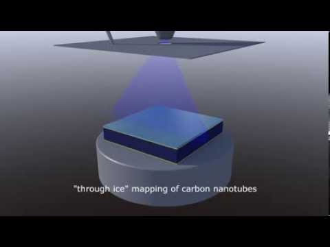
Carbon Nanotube FET fabrication using Ice Lithography
0:06:34
Kafai Lai: Exploring technology solutions with computational lithography
0:15:35
EUV Lithography. But With a Free Electron Laser
0:18:51
How Extreme Ultraviolet Lithography works | Part 1/3
0:10:39
Eulitha Lithography for Photonics, nanolithography services/equipment for research and production
0:18:40
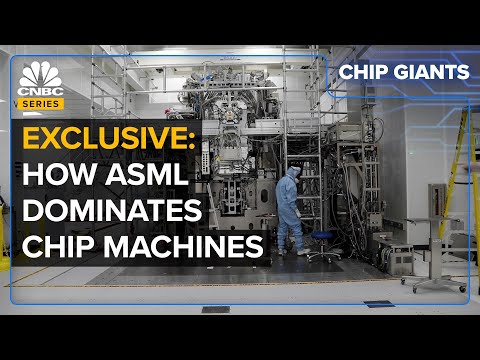
Why The World Relies On ASML For Machines That Print Chips
0:25:33
Japan’s EUV Failure
0:03:17
VLOG-245 | The #Semiconductor Computational Lithography Career
1:05:06
A brief introduction to e-beam lithography
0:28:23
Tech Talk – Inverse Lithography Technology (ILT): 30 Years to Full-Chip Reality, Spring Edition 2022
0:20:39
Determining the Resolution Limits of Electron-Beam Lithography
0:36:13
Hakaru Mizoguchi: Development of 250W EUV Light Source for HVM Lithography
0:09:59
China's Breakthrough in Lithography Technology for Semiconductor Manufacturing #semiconductor
0:18:23
Etch: Lithography's Unheralded Sibling
Вперёд
visit shbcf.ru
 0:07:44
 0:05:26
 0:01:37
 0:06:08
 0:06:35
 0:06:22
 1:14:34
 0:08:16
 0:18:51
 0:00:23
 0:02:01
 0:06:34
 0:15:35
 0:18:51
 0:10:39
 0:18:40
 0:25:33
 0:03:17
 1:05:06
 0:28:23
 0:20:39
 0:36:13
 0:09:59
 0:18:23